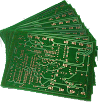
Generally, a printed circuit board that is homemade is done by printing the layout in a suitable transparent medium. The printed layout is exposed to a photoresist chemical so that the pattern is copied on the PBC followed by moving the transparent design to the printed circuit board by using ultra violet light, then using developer to develop the circuit pattern on the printed circuit board, then etching the pattern, washing the PBC and washing with water, drilling holes, and finally drilling, mounting, and soldering the components.
This article will give you some input on how you can simplify the process by bringing about a change in the layout and design phase. It helps in reducing the cost of carrying out the in-house making of a PBC. These tips will help in reducing the time needed to complete a printed circuit board and also eliminates previous issues of developer chemical, ultra violet lights, etc.
Printed circuit board layout: By using CAD softwares like Protel, Orcad, etc. the layout of the circuit board can be made. Different PBC layouts are also available different electronics magazine.
If you are interested in doing the layout yourself, then first draw the schematics followed by the printed circuit board layout. Apart from Protel and Orcad, there are other softwares that are also available in the market. However, care should be taken in selecting the right software in order to make sure that you don't land with a software that has limited functions.
Design rule for a printed circuit board
Before deciding on the layout of a printed circuit board, a lot of thought must be given to the cost and the reasonableness of making an in-house printed circuit board.


Thanks for informative post. I am pleased sure this post has helped me save many hours of browsing other similar posts just to find what I was looking for. Just I want to say: Thank you!
BeantwoordenVerwijderenPCB Manufacturing