woensdag 13 april 2011

Printed Circuit Board: Tips on the layout and design


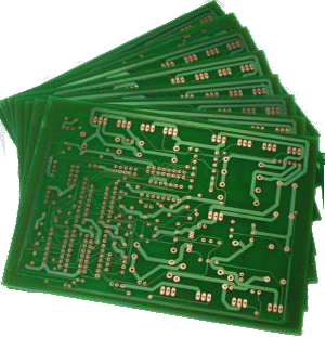
Generally, a printed circuit board that is homemade is done by printing the layout in a suitable transparent medium. The printed layout is exposed to a photoresist chemical so that the pattern is copied on the PBC followed by moving the transparent design to the printed circuit board by using ultra violet light, then using developer to develop the circuit pattern on the printed circuit board, then etching the pattern, washing the PBC and washing with water, drilling holes, and finally drilling, mounting, and soldering the components.

This article will give you some input on how you can simplify the  process by bringing about a change in the layout and design phase. It helps in reducing the cost of carrying out the in-house making of a PBC. These tips will help in reducing the time needed to complete a printed circuit board and also eliminates previous issues of developer chemical, ultra violet lights, etc.

Printed circuit board layout: By using CAD softwares like Protel, Orcad, etc. the layout of the circuit board can be made. Different PBC layouts are also available different electronics magazine.

If you are interested in doing the layout yourself, then first draw the schematics followed by the printed circuit board layout. Apart from Protel and Orcad, there are other softwares that are also available in the market. However, care should be taken in selecting the right software in order to make sure that you don't land with a software that has limited functions.

Design rule for a printed circuit board

Before deciding on the layout of a printed circuit board, a lot of thought must be given to the cost and the reasonableness of making an in-house printed circuit board.

Printed Circuit Board: How it Happened


A printed circuit board is a fundamental part of electronic devices, and it helps in assembly of intricate parts within a small space. Though a little expensive in the initial design phase, in the long run printed circuit board has reasonable manufacturing cost and are very sturdy. They last for a long time. In the beginning, printed circuit boards were used in radios during World War II. Later it graduated to the commercial level and has evolved since then.

History

As per the U.S. Patent, in July 31, 1956, M. Abramson got the patent rights for a printed circuit board although it was an Austrian Who first made the printed circuit board in England. The printed circuit board came into existence due to the efforts of an Austrian engineer named Paul Eisler , which was used as part of a radio set. By 1943 this impressive innovation was being used by the U.S to make rugged radios that were used in World War II. Post World War II, the US started using this technology for commercial use. However, it was quite a while before the printed circuit board was more commonly used in commercial electronic goods.

 From the second half of the 19th century, the connecting parts like components and wiring of an electrical device was done on a wooden board. It was only in the 20th century that printed circuit boards were developed that had the circuit etched on the surface of the board.

Advantage of a printed circuit board

A printed circuit board reduces the manufacturing cost, offers a very efficient and compact way of wiring, and placement of more components in a limited space.

The future

The need of the modern technology is compactness and miniaturization that leads of the decrease in the size of the components and increasing the number of patterns on a printed circuit board. Hence, in the long run another approach may be required to meet this requirement as there is a limit on how close the printed wires can exist.


Homemade Printed Circuit Board


In order to make a homemade printed circuit board for prototyping, the materials required are:

  1. Copper board: Copper clad boards are obtainable in various sizes, and the right size will be the one which can fit all the components. The copper coated side of the board will be used for soldering while the other side will be used for adding the components.
  2. Solution of Ferric chloride: It is an etching solution that eliminates unwanted layers of copper from the copper clad board. To make this etching solution, dissolve 50 gms of Ferric chloride powder in 100 ml of warm water.
  3. Drilling holes: For drilling holes on the board,  a printed circuit board drills or hand drill with the relevant bits is enough for the purpose.

Making the printed circuit board

  1. First draw the circuit in a compact manner on a piece of paper. Mark the places where the components would be drilled.
  2. Draw this same diagram on a tracing or a butter paper with the help of a OHP marker pen.The reverse side of the drawing paper will be the actual design of the printed circuit board.
  3. Place the pencil carbon paper on the copper side of the board.
  4. Put the paper containing the design sketch over the carbon paper.
  5. Redraw the design so that the carbon ink traces the design on the copper board.
  6. Remove the papers and redraw the design on the  carbon board by fowwing the trace left by the carbon paper on the copper board.
  7. Identify the locations which needs to be drilled.
  8. Place the copper board on a porcelain or plastic tray and pour ferric chloride solution till the board submerges in it. 
  9. Expose the tray to sunlight and shake it a number of times. Etching will be done in two hours.
  10. Clean the board with water.
  11. Drill the holes.
  12. Get rid of the pen markings by using thinner.
  13. Solder the tracks.

Warning: As ferric chloride is harmful, avoid its contact with your skin.